The Transistor: The Invention That Made Everything Else Possible
Abstract
On December 16, 1947, two physicists at Bell Laboratories demonstrated a device so small it fit in the palm of a hand, yet so consequential that every computer, smartphone, and electronic device in existence today descends from it. The transistor (invented by John Bardeen and Walter Brattain, with crucial theoretical work by William Shockley) replaced the fragile, power-hungry vacuum tube with a solid-state switch that could be made smaller, cheaper, and more reliable with each passing year. The three men shared a Nobel Prize in 1956, by which time they had long since stopped working together. The transistor united a field; it divided the men who created it.
The Problem with Glass
By the mid-1940s, electronic computers existed, but they were monsters. The ENIAC, completed in 1945, used nearly 18,000 vacuum tubes and filled a large room at the Moore School of Electrical Engineering at the University of Pennsylvania. It consumed 150 kilowatts of power, generated enough heat to warm a house, and stopped roughly every two days when one of its thousands of tubes burned out.
The vacuum tube was a triumph of 1910s engineering that had reached its fundamental limits. It worked by heating a metal filament inside a glass envelope until electrons boiled off and could be steered by an electric field, exactly the same principle as an incandescent light bulb, just harnessed for switching and amplification rather than illumination. But heating filaments took time and energy. Glass envelopes broke. Tubes that ran hot enough to work reliably also wore out quickly.
The engineers who designed ENIAC understood perfectly that vacuum tubes were a dead end. What nobody knew was what would replace them. See From Vacuum Tubes to Transistors for the broader context of this transition.
Bell Labs and the Solid-State Group
In 1945, Mervin Kelly, research director at Bell Telephone Laboratories in Murray Hill, New Jersey, assembled a team to investigate solid-state alternatives to the vacuum tube. Bell Labs had both the motive and the means: AT&T’s telephone network depended on millions of vacuum-tube amplifiers in its long-distance lines, and every tube that failed required a technician. A solid-state amplifier with no moving parts, no filament, and no glass envelope would transform the economics of the entire telephone system.
Kelly chose William Shockley to lead the group. Shockley was brilliant, ambitious, and difficult, a theoretical physicist who combined genuine insight with a compulsive need for personal credit. He surrounded himself with people whose abilities complemented his own: John Bardeen, a quiet, methodical theorist trained at Wisconsin and Princeton who had a gift for understanding the quantum mechanics of surfaces, and Walter Brattain, a hands-on experimentalist who had spent his career probing the electrical behavior of semiconductor materials.
The three men were an unlikely team. Bardeen was self-effacing to the point of invisibility; colleagues sometimes forgot he was in the room until he spoke and said something brilliant. Brattain was a craftsman, more comfortable with a soldering iron than a blackboard. Shockley was the manager, the theorist, and (in his own accounting) the creative engine. He would eventually be proved, partly, wrong about that last part.
December 16, 1947
Through late 1947, Bardeen and Brattain worked together on a specific experimental approach: pressing metal point contacts against a germanium semiconductor surface and probing what happened when small voltages were applied. Shockley had predicted that a field applied above the surface would control current flow through the material. The experiments kept failing in ways that Shockley’s theory could not fully explain.
On December 15 and 16, 1947, Bardeen and Brattain made it work. Their device (two gold foil contacts pressed against a germanium crystal mounted on a metal plate) could amplify a signal. When a small current flowed through one contact, it controlled a much larger current through the other. They had created the point-contact transistor, and on 23 December 1947 they demonstrated it to Bell Labs management. The name “transistor” came later, from an internal vote in 1948.
Shockley was not in the room. This fact would gnaw at him for years. He had led the group, defined the program, and provided theoretical direction, but the breakthrough had happened while he was elsewhere, and his name was not on the initial patent application.
His response was characteristically Shockley: within weeks, working alone in a hotel room in Chicago in January 1948, he developed the theory for an entirely new and superior device, the junction transistor, which replaced the fragile metal points with layers of differently doped semiconductor. The junction transistor was more reliable, more manufacturable, and more powerful than the point-contact version. It was the design that would actually be mass-produced.
The Announcement and Its Aftermath
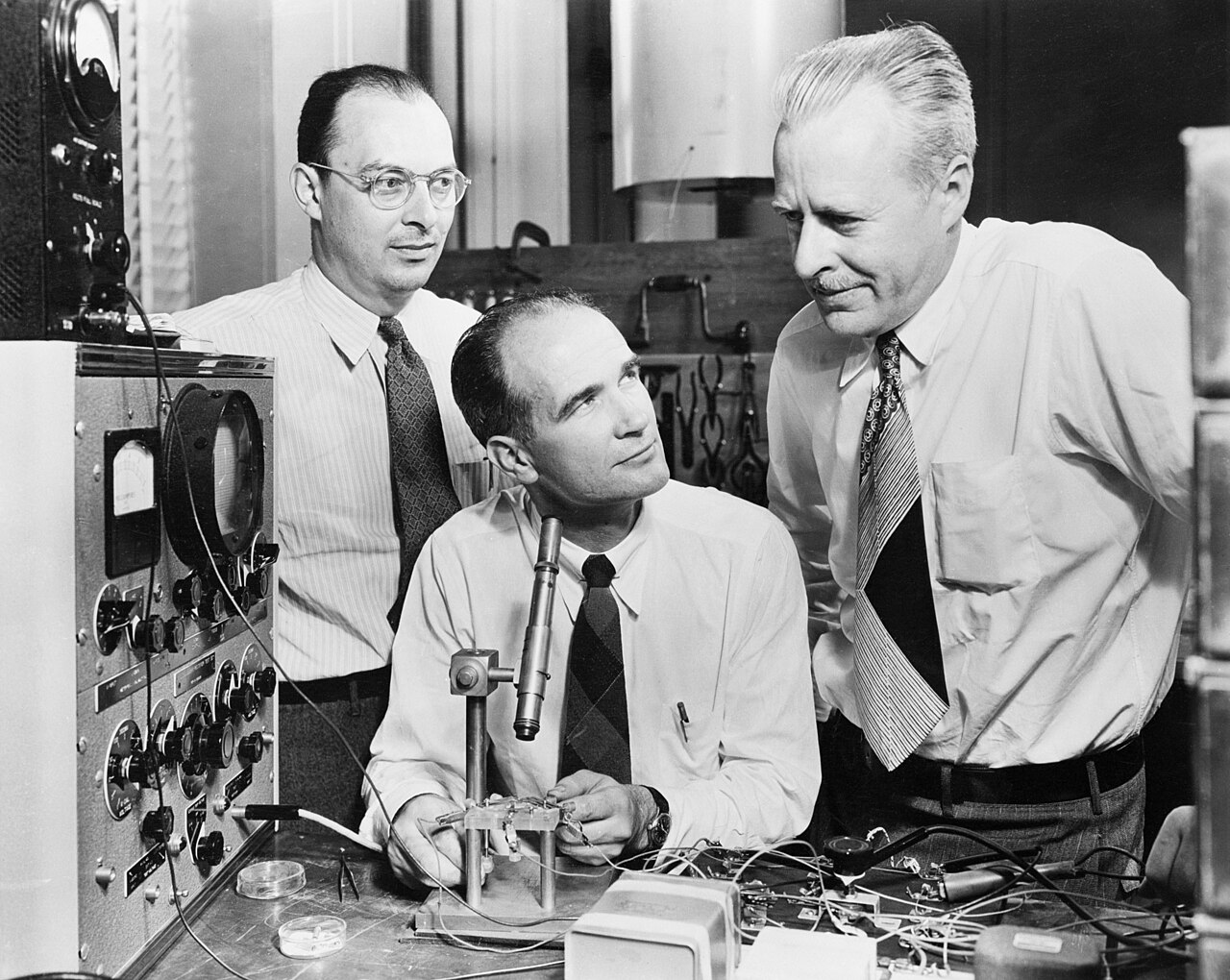
Bell Labs management recognized the significance of the discovery but moved cautiously. The transistor was kept secret for six months while lawyers filed patents and engineers explored implications. Bardeen and Brattain’s paper appeared in Physical Review that summer. On June 30, 1948, Bell Labs’ research director Ralph Bown announced the invention at a press conference in New York; Shockley sat at the centre of the best-known publicity photograph, peering into a microscope. The New York Times covered it on page 46, a brief item in the radio news column. The world had not yet understood what had happened.
Bell Labs held licensing seminars throughout the early 1950s, charging a modest $25,000 fee to any company that wanted to learn transistor manufacturing technology. The policy was partly practical (Bell needed partners to develop manufacturing techniques) and partly mandated: AT&T’s regulated status made hoarding the technology legally awkward. The seminars seeded the transistor into dozens of companies across the United States and Japan. One of the attendees was from a small company then called Tokyo Tsushin Kogyo, led by Masaru Ibuka; it went home and built Japan’s first transistor radio (the TR-55, 1955), a year after the American Regency TR-1 had become the world’s first commercial transistor radio. The company eventually became Sony.
The French Transistron
The transistor was invented twice. Two German physicists, Herbert Mataré, a former Telefunken radar researcher, and Heinrich Welker, who had developed a germanium rectifier for Siemens, set up a semiconductor laboratory in 1947 for the Compagnie des Freins et Signaux Westinghouse in an empty house at Aulnay-sous-Bois near Paris. Working on germanium diodes, Mataré found that a weak current at one contact controlled a stronger one at another, and on 13 August 1948 the two filed a French patent for a “new crystal system with several electrodes producing electronic relay effects,” apparently without knowledge of the Bell Labs work. The French post and telecommunications ministry presented it on 18 May 1949 as the transistron; about a thousand were made that year before production lapsed. Mataré went on to run Intermetall in Düsseldorf from 1952 and Welker the semiconductor research of Siemens in Erlangen from 1951. The theory both teams relied on owed much to Walter Schottky’s work at Siemens in the 1930s, and Julius Lilienfeld had patented the principle of the field-effect transistor in 1925.
The Nobel Prize and Three Men Who Couldn’t Speak
In 1956, Shockley, Bardeen, and Brattain were awarded the Nobel Prize in Physics “for their researches on semiconductors and their discovery of the transistor effect.” By then the three had not worked together for years.
Shockley’s behavior had become increasingly abrasive throughout the early 1950s. He took credit aggressively, excluded colleagues from key meetings, and managed through intimidation. Brattain had asked to be moved out of Shockley’s group, and Bardeen left Bell Labs in 1951 for the University of Illinois. Bardeen went on to win a second Nobel Prize in 1972 for superconductivity theory, still the only person to have won the Nobel Physics Prize twice.
Shockley Semiconductor and the Traitorous Eight
In 1956, flush with the Nobel Prize and convinced he could run a company better than Bell Labs, Shockley moved back to Palo Alto, California, where he had grown up, and founded Shockley Semiconductor Laboratory, the first semiconductor company in what would eventually be called Silicon Valley. He assembled a team that was, by any measure, extraordinary: Robert Noyce, Gordon Moore, Jean Hoerni, Julius Blank, Eugene Kleiner, Jay Last, Victor Grinich, and Sheldon Roberts.
Shockley then proceeded to manage them exactly as he had managed at Bell Labs. He subjected employees to lie detector tests when a minor accident occurred. He announced salary information without consent. He redirected the company’s technical program away from silicon transistors toward a more exotic device that most of the engineers considered unpromising. He was, by all accounts of the people who worked for him, brilliant and impossible in equal measure.
In 1957, all eight engineers resigned simultaneously to found Fairchild Semiconductor with backing from Sherman Fairchild. Shockley called them the “Traitorous Eight,” a phrase he intended as condemnation that history has worn as a badge of honor. From Fairchild, Noyce’s planar integrated circuit followed within two years (Jack Kilby had built his independently at Texas Instruments in 1958). From Fairchild’s diaspora, Intel (founded by Noyce and Moore in 1968) arose a decade later. See The Integrated Circuit Revolution and Gordon Moore and Moore’s Law for the sequels to this story.
Shockley’s company never produced a commercially successful product. He eventually left the semiconductor business and spent his later years promoting theories about race and intelligence that destroyed his scientific reputation. He died in 1989, estranged from his children.
Germanium to Silicon
The first transistors used germanium, the semiconductor material Bardeen and Brattain had experimented with. Germanium worked, but it had a fundamental weakness: it degraded at temperatures above about 75°C, which made it unsuitable for applications involving heat, including many of the military electronics applications that drove early transistor demand.
Silicon, the second most abundant element in the Earth’s crust, had better high-temperature properties but was much harder to purify and process. Through the early 1950s, researchers at Texas Instruments (where Gordon Teal had moved after leaving Bell Labs) and later at Fairchild developed the techniques needed to make silicon transistors practical. Teal had applied Jan Czochralski’s 1916 crystal-pulling method to germanium at Bell Labs in 1948; as research director at TI from 1953 he set Willis Adcock’s team to grow silicon crystals, and their first silicon transistor worked on 14 April 1954. Morris Tanenbaum at Bell Labs had made one in January 1954 but kept it quiet. At an electronics conference in Dayton on 10 May 1954, after speakers had predicted years of delay, Teal played a record through an amplifier, dropped its germanium transistor into hot oil and the music stopped, then repeated the test with a silicon transistor and the music played on; listeners ran for the telephones. Texas Instruments also put the transistor into consumers’ hands: it financed the Regency TR-1, built by I.D.E.A. of Indianapolis, announced on 18 October 1954 and on sale from 1 November at $49.95. It sold about 140,000.
Fairchild’s crucial contribution was the planar process, developed by Jean Hoerni in 1959: a method of building transistors by diffusing dopants through openings in a protective oxide layer on a flat silicon surface, instead of etching raised three-dimensional structures. The planar process made transistors manufacturable with photographic precision, enabling the yields and miniaturization that the integrated circuit required. Silicon became the universal substrate; germanium faded from the industry.
The Field-Effect Path
The transistor Bardeen and Brattain demonstrated in 1947 is not the transistor the world runs on today. Modern chips are built from a different device, the field-effect transistor, whose history is longer and stranger: the concept was patented two decades before the point-contact transistor and became practical only thirteen years after it.
In 1926, the Austro-Hungarian physicist Julius Edgar Lilienfeld filed a US patent for a three-electrode amplifier using copper-sulfide semiconductor material, the field-effect principle in recognizable form (a Canadian filing had preceded it in 1925, a second US patent followed in 1928). There is no evidence he ever built a working device, and with the materials of the 1920s he almost certainly could not have: the effect depends on semiconductor surfaces of a purity nobody could then produce.
Shockley’s own field-effect experiments at Bell Labs from 1945 failed for exactly that reason. Electrons trapped at the semiconductor surface (the “surface states” Bardeen described theoretically) screened out the applied field. The point-contact transistor emerged from the effort to understand this failure; the field effect itself remained out of reach.
The problem fell in 1959 and 1960, at Bell Labs again. Mohamed Atalla had found that growing a thermal silicon-dioxide layer on silicon passivated the surface and tamed the surface states. Together with Dawon Kahng he used this oxide as an insulated gate and demonstrated the first working MOSFET (metal-oxide-semiconductor field-effect transistor) in 1960. Bell Labs looked at the result and passed: the device was slower than bipolar transistors and answered no pressing need of the telephone system.
Others picked it up. In 1960, Karl Zaininger and Charles Meuller fabricated a MOS transistor at RCA, and C.T. Sah at Fairchild built a MOS-controlled tetrode; in 1962, Fred Heiman and Steven Hofstein followed with an experimental 16-transistor integrated MOS device at RCA. The first commercial parts arrived in 1964: p-channel devices from General Microelectronics (GME 1004) and Fairchild (FI 100) for logic and switching, an n-channel transistor from RCA (3N98) for amplification. In 1963, Frank Wanlass and Chih-Tang Sah at Fairchild described CMOS, the complementary MOS circuit that draws power only while switching and that practically all digital chips use today.
What the MOSFET gave up in speed it returned in manufacturability. Simpler and smaller than the bipolar transistor, and frugal with power in its CMOS form, it became the device that scaling actually happened to: the first microprocessors of 1971 were MOS chips, and every processor, memory chip, and smartphone since is a collection of MOSFETs. By 2018, an estimated 13 sextillion transistors had been manufactured, 99.9 percent of them MOS devices, which makes the MOSFET the most produced artifact in human history.
Why Everything Changed
The transistor’s advantages over the vacuum tube were not incremental; they were categorical:
Size: The first transistors were roughly the size of a peanut. Vacuum tubes were the size of a thumb. By the 1960s, transistors were being measured in micrometers. Today, the features of transistors in a modern processor are measured in nanometers, a few dozen atoms across.
Power consumption: A vacuum tube required continuous power to heat its filament. A transistor needed no heater and ran on milliwatts. A computer with transistors instead of tubes consumed a fraction of the energy.
Reliability: A vacuum tube’s filament would eventually burn out, just like a light bulb. A transistor with no heated filament had no comparable failure mechanism. Solid-state devices measured their mean time between failures in decades, not hours.
Cost and scalability: Vacuum tubes were hand-assembled glass objects, each one individually manufactured. Transistors could eventually be etched onto silicon wafers by the thousands, then millions, then billions, using photographic techniques that scaled cheaply.
Every integrated circuit is a collection of transistors. Every microprocessor is an integrated circuit. The Intel 4004, introduced in 1971, contained 2,300 transistors. The largest Apple M-series chips contain more than 100 billion. The device that Bardeen and Brattain demonstrated in Room 1E455 at Bell Labs on December 16, 1947, was not one invention among many. It was the invention that made all the others possible.
📚 Sources
- Heinz Nixdorf MuseumsForum blog, “Die Geburt des Transistors” (22 December 2017)
- Heinz Nixdorf MuseumsForum blog, “Die zweite Geburt des Transistors” (13 August 2018)
- Heinz Nixdorf MuseumsForum blog, “Willkommen im Silizium-Zeitalter” (28 March 2022)
- Heinz Nixdorf MuseumsForum blog, “Es begann mit Regency” (1 November 2024)
- Riordan, Michael & Hoddeson, Lillian — Crystal Fire: The Invention of the Transistor and the Birth of the Information Age (1997)
- History of the transistor — Wikipedia
- Nobel Prize — Physics 1956: Bardeen, Brattain, Shockley
- Gertner, Jon — The Idea Factory: Bell Labs and the Great Age of American Innovation (2012)
- Shurkin, Joel — Broken Genius: The Rise and Fall of William Shockley (2006)
- Computer History Museum — Transistor Milestone
- The Traitorous Eight — Wikipedia
- Bardeen, John — Nobel Lecture, December 11, 1956
- Computer History Museum — 1926: Field Effect Semiconductor Device Concepts Patented (Lilienfeld)
- Computer History Museum — 1960: Metal Oxide Semiconductor (MOS) Transistor Demonstrated
- Computer History Museum — 13 Sextillion & Counting: The Most Frequently Manufactured Human Artifact in History (2018)
- MOSFET — Wikipedia